Engineers have tried to battle Electrostatic Discharge (ESD) for a long time now, as it can cause actual damage to your electronics. Nobody wants their equipment to stop functioning properly because somebody carelessly walked across a room in the middle of winter, on a carpeted floor, wearing a polyester jacket, brushing their hair with a PVC pipe and then decided to touch some doomed electronics! How dare they!? Haven't they heard of wearing a ground strap 24x7?
Jokes apart, the electronics industry has come up with tests and standards that components and products are recommended to meet in order to ensure ESD will cause no harm to the brave electronics that go forth into the world. Now, you also don't want your product's launch held up because your ESD protection circuit design was a little sloppy.
I learnt a whole lot to do with designing for ESD immunity when working on a product and bringing it to the hands of costumers.
As a EE system designer, are you wondering...
- How is ESD characterized? There are many different notations, but which is the most important?
- So many different levels of ESD immunity! What do they actually mean? What level of immunity should I try to achieve?
- How to design my ESD protection circuit? How to avoid a last minute redesign?
If you are interested in any of these questions... READ ON!
Section 1: Understanding Different ESD Standards
ESD as it relates to discharges into electronic components, are denoted with many different models. This is because, the ESD energy profile and waveform varies largely based on the particular discharge environment.
1.1 ESD standards for component level immunity in the manufacturing environment:
External charge is delivered by a human body to the device. Voltages are in the range of 1 kV – 10 kV.
Charged Device Model (CDM):
Electronic device itself gets charged by electrostatic induction and later discharges to an outside object. Voltages are in the range of 200 V – 2000 V
Machine Model (MM):
External charge delivered by a machine (metal). Voltages are in the range of 100 V – 200 V. The stress level of MM is approximately 10 times lower than that of HBM discharge.
Here is a graph showing how the discharge curves of the different models are very different from each other.
CDM, MM, and HBM ESD current versus time graph 1
1.2 ESD standards for system level immunity in the real world:
IEC61000-4-2 ESD standard:
IEC61000-4-2 is a standard that was established to provide a common and reproducible basis for evaluating the performance of electronic equipment when subjected to ESD. The ESD strike designed under this standard is a lot more rigorous than all the models described above.
IEC61000-4-2 waveform is designed with exact specifications on the shape 2
Comparison of the IEC waveform with HBM and CDM waveforms 3
1.3 Are the HBM, CDM, MM models relevant? Not for a system level designer!
System level designers should only be focused on the IEC61000-4-2 immunity. HBM, CDM and MM models are designed to only test component level performance within the scope of a specific environment. While, this data is useful for PCB assembly houses and factory floors that handle these ICs, it does not guarantee any immunity to ESD out in the real world. The IEC standard is more rigorous: faster rise time, longer duration, higher peak pulse current and significantly more energy! This is only standard that ensures system-level immunity.
Screenshot from a datasheet 4
For e.g., the datasheet of a Cypress PSoC component talks about how the IC is resistant to 2200 V of HBM and 500 V of CDM style ESD discharge. After seeing this, do not fall into the trap of thinking that some level of ESD immunity is built into the device and miss adding extra ESD protection to the pins of this IC that may be exposed to the outside world (via a connector, etc.).
Beware of misleading marketing specifications calling out "integrated ESD protection" and always double check which standard the immunity has been tested against. If you see an IEC level immunity listed on a datasheet, only then can you consider trusting the immunity built-in. It might still need extra protection devices, based on which IEC level of immunity you are trying to achieve.
Section 2: Diving deeper into IEC61000-4-2 standard
Now that we have established that the IEC61000-4-2 is the most important standard, let's understand a little bit more. The IEC standard establishes 4 different levels or classes of immunity.
The level or class of immunity you are trying to design for, depends on what your product requires depending on what type of environment it will be used in. For consumer grade equipment that will be constantly touched by people, for e.g. a laptop, you will want to aim to achieve class 4 immunity.
Testing for the IEC standard is usually conducted with a ESD test gun on a proper test table. There are two types of discharges under each class - Air and Contact. Be sure the select the right style of probe tip on the ESD gun.
Top: Contact discharge tip / Bottom: Air discharge tip
Contact discharge involves discharging an ESD pulse directly from the ESD test gun that is touching the device under
test. In the air discharge test, the ESD test gun is
brought close to the device under test until a discharge occurs. The standards are defined so that each level's air or contact discharge is
considered equivalent.
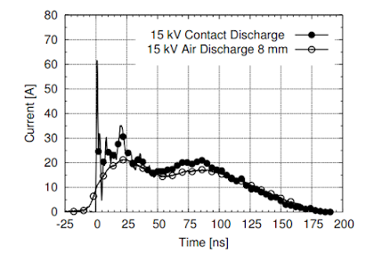
Generally, the preferred method of testing is the contact discharge test, because it is more rigorous than the air discharge. As a rule of thumb, contact discharge test at a certain voltage almost always guarantees immunity against an air discharge at the same voltage.
Contact vs. Air discharge waveform shows that contact has higher transient voltage 5
In an air discharge, the initial high voltage peak is consumed by the arc to just jump from the ESD test gun to the device under test.
Section 3: Designing ESD protection
3.1 Prevent entry of ESD strike
The best way to prevent an ESD event from occurring in the first place is to have a proper enclosure made of insulating material like plastic, to cover the entire electronic product. However this is not possible in most products, as they will have exposed conducting surfaces like connectors or port, or holes like air vents or screw holes that expose the PCB inside. Do the best possible.
3.2 ESD protection circuit
Here is the most comprehensive ESD protection circuitry that I believe covers almost all the components you will ever need :
Shunt Capacitor, Shunt TVS (transient voltage suppression) Diode, Series Resistor.
Note, you do NOT need all of these components for every instance of protection circuitry. You have to pick and choose one or more of these three components, based on a case-by-case basis. Generally place these components in the same order between the connector and IC as shown here.
For many instances having the series resistor or the decoupling capacitor will not be appropriate since that might ruin the functionality of that trace, e.g. high speed data trace with a controlled impedance and low stray capacitance requirement.
Let's look at how and when each of these components are useful.
TVS Diode:
The main protection device is obviously the TVS, Transient Voltage Suppression, diode. This is essentially a Zener diode that stays in reverse bias most of the time, but breaks down and starts conducting under the high voltage of an ESD strike. Usually it is best to use a bidirectional TVS that will conduct under a high positive or negative voltage strike.
ESD event suppressed by TVS diode 6
Things to keep in mind:
- TVS diode clamping voltage: Once the TVS diode conducts, it will only bring the voltage down to the rated clamping voltage, which can be in the range of 10-50V. Make sure the downstream IC can handle this clamping voltage transient. If the IC gets into a latch up state, or is harmed in any other way by the transient voltage, one needs to find either a different ESD diode or add in extra protection such as a series resistor.
- How do I know the clamping the voltage for my TVS diode - at different levels of IEC waveform ESD strikes? Either read a TLP graph or look at the datasheet. More on this in another blog post.
- TVS diode working voltage: The diode should not conduct under normal operation of the trace it sits on, with added margin. This also includes choosing the right polarity and bi-directionality if needed for the diode.
- TVS diode stray capacitance: Adding a TVS diode will add a little extra capacitance on the PCB trace. This will be a problem with high speed signal with fast requirements on rise and fall times. Watch out and choose an appropriate TVS diode with low stray capacitance.
Series Resistor:
In some instances, a series resistor might be required to limit the current flowing into the pin of the IC, if the clamping voltage of the TVS diode is still high enough to cause significant current inrush into the IC. Make sure this resistor is placed after the TVS diode and not before, on the ESD path. A resistor without the TVS diode's clamp does very little in the face of high voltages of an ESD. The voltage arc will usually jump right across a 0402 resistor.
Determine the value of the series resistor based on clamping voltage, max. current the IC can handle and max. resistance the trace can handle under normal operation.
Decoupling Capacitor:
Capacitors provide decoupling and can help absorb the ESD strike's energy, while shunting the transient events to ground. It’s best to choose capacitors with high voltage ratings, high resonant frequency, low resistance and low inductance. Make certain to minimize trace lengths when connecting capacitors.
One can place the capacitor before or after the TVS diode on the ESD path.
A series inductor before the TVS diode is sometimes useful in blocking high currents from an ESD strike, but that also means, a higher voltage will be induced across the inductor and add the voltage from the ESD strike, so inductors must be used with caution.
There is also a myth that ferrite beads being place before the TVS diode can help with ESD suppression, but this is not true. The frequency of an ESD strike is upwards of 2 GHz (the first peak), and a ferrite bead will usually let that pass through will not much impedance. Even if it did present a significant impedance at that frequency, the ESD can just arc across the component.
3.3 Layout Guidelines
After figuring out all the different components that will go into your protection circuitry, the last piece of the puzzle is to carefully review the PCB layout to ensure the component placement is optimal for ESD immunity. Optimizing a PCB layout for ESD suppression is largely dependent on designing the path to ground for the ESD current.
- Place the TVS diode as close as possible to the point of entry of the ESD strike.
- Route with straight traces between the ESD entry point and the TVS if possible. Else use rounded curves or 45 degree curves at the most.
- Place the protected IC further away from the TVS diode.
- Do not use stubs between the TVS and the protected trace, instead route directly to the TVS and then to the rest of the system from there. Ensures the TVS can first suppress the ESD strike before it can reach the protected IC.
- Ensure there are enough ground vias near the TVS to enable minimum impedance. Adding any trace inductance on the ground side of the TVS will result in a significant voltage being seen across that inductance during an ESD event.
- Avoid vias between the ESD entry point and TVS if possible. If a via is required, route directly from the ESD
entry point to the TVS before using the via to the protected IC. This ensures the ESD current will not experience a via stub between the protected trace and TVS.
- Ensure all vias on the ESD path are of the largest diameter, depending on the design constraints.
- In order to minimize EMI / ESD jump into other unprotected traces on the board. Do not route unprotected circuits in the area between the ESD entry point and the TVS diode.
EMI coupling onto an adjacent unprotected trace 7
Guideline for a trace with a via 7 Conclusion
To successfully design an ESD protection circuit for a system:
- Understand the standards and always aim to achieve IEC61000-4-2 standard immunity. Do not be confused with the component level standards.
- Decide which class of ESD immunity is required for your product early on in the design phase.
- Contact discharge immunity usually also means air discharge immunity at the same voltage level.
- Carefully note all the different system parameters and design an ESD protection circuit by choosing a TVS and using other components like series resistor, decoupling capacitor, etc. if needed. Note things like TVS turn-on time, stray capacitance, TVS clamping voltage. Every detail matters.
- Optimize PCB layout to help ESD find the shortest path to ground.
All the best. Hope you find this blog post useful.
Sources Footnotes:
1: https://www.embedded-computing.com/guest-blogs/fundamentals-of-hbm-mm-and-cdm-tests
2: https://www.silabs.com/documents/public/application-notes/AN895.pdf
3: https://m.eet.com/media/1163218/3547-esd_device_testing_the_test_determines_the_result.doc
4: https://www.cypress.com/file/302286/download
5: https://www.armms.org/media/uploads/03_armms_nov12_wsimbuerger.pdf
6: https://www.ti.com/lit/sg/sszb130c/sszb130c.pdf
7: https://www.ti.com/lit/an/slva680/slva680.pdf